Our Research
Metal halide perovskite photovoltaics: performance and stability
We are interested in routes to improving the performance and stability of metal halide perovskite photovoltaics. Our work looks at how different fabrication approaches and chemical changes influence device performance. Some of our recent work in this are can be found through the following links:
Thermally stable passivation toward high efficiency inverted perovskite solar cells
A piperidinium salt stabilizes efficient metal-halide perovskite solar cells

Wide band gap perovskites
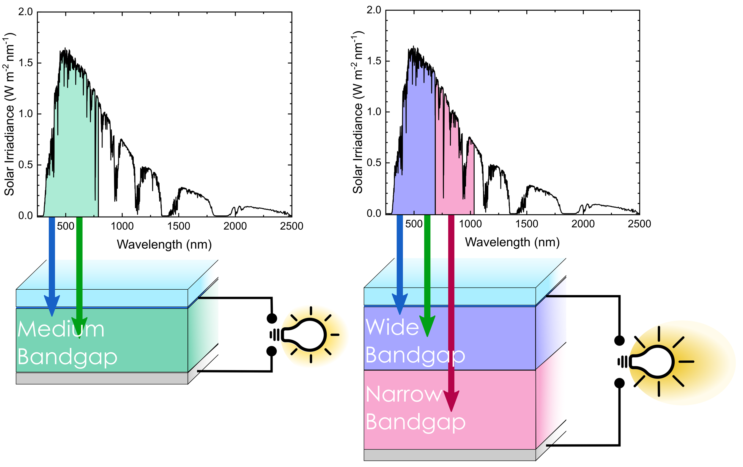
There are thermodynamic limits to how efficient solar panels with one absorber layer can be - this is often known as the radiatiave limit.* One way we can circumvent this limit is by coupling two solar absorber layers (one with a low and one with a high bandgap) to form a tandem photovoltaic. Metal halide perovskites are particularly attractive for these applications however wide bandgap perovskite photovoltaics suffer from voltage losses (the causes of which are currently unknown) which limit how efficient they can be.
We study the origin of these voltage losses - investigating the charge carrier recombination in these materials (through photoluminesence spectroscopies) and at the interfaces between the perovskite and other charge transporting layers in photovoltaic devices. We combine this understanding with photoemission studies to probe the energy level positions of these semiconductors and explore routes to reducing these voltage losses in photovoltaic devices.
*please see this article on the naming of this phenomenom
Our recent papers on this topic can be found through the following links:
REVIEW: Methylammonium-free wide bandgap metal halide perovskites for tandem photovoltaics
Tandem photovoltaics can harvest more of the solar spectrum than a single junction photovoltaic. More light absorbed can lead to higher sunlight to energy conversion.
Imaging surface and electrical properties of semiconductors
In any optoelectronic device there are several interfaces between its components. Changes in crystal structure, morphology and electronic structure can all impact the charge carrier transport through a device. Understanding these interfaces is critical to boosting device performance.
We use a range of different techniques to study semiconductor surfaces. Scanned probe microscopy allows us to investigate the morphology of our surfaces. Photoemission spectoscopies allows us to investigate the chemistry and electronic structure of these surfaces. Diffraction allows us to study the crystal structure of our surfaces. All of this knowledge allows us to design more efficient optoelectronic devices.
Some of recent papers on this topic can be found through the following links:
Thermally stable perovskite solar cells by all-vacuum deposition
Revealing the stoichiometric tolerance of lead trihalide perovskite thin films

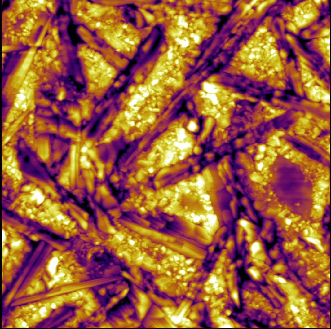
Atomic force microscopy images of different metal halide perovskite thin films.